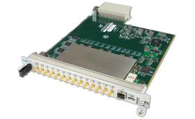
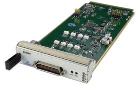
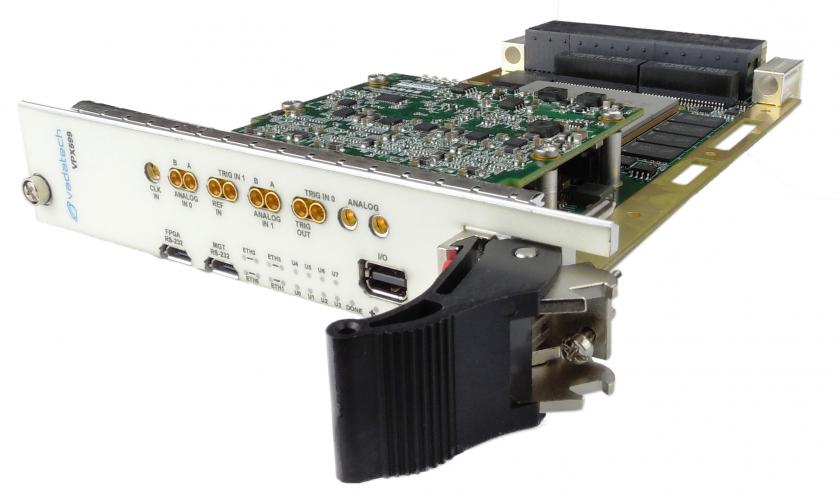
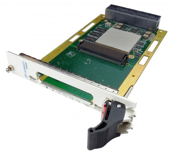
VPX589
- (similar products)
- VPX599 - Dual ADC @ 10.4 or 6.4 GSPS and Dual DAC @ 12 GSPS, UltraScale™, 3U VPX
- VPX597 - 300 MHz to 6 GHz Octal Versatile Wideband Transceiver (MIMO), Kintex UltraScale™, 3U VPX
- VPX598 - Quad DAC @ 12 GSPS with Quad ADC @ 3 GSPS, Kintex UltraScale™, 3U VPX
- VPX570 - ADC 12-bit @ 5.4 GSPS and DAC 12-bit @ 6 GSPS, Virtex UltraScale+, 3U VPX
- VPX571 - Dual RF Agile Transceiver with VITA 67.2 RF Connector, 3U VPX
- MPM_VPX570 - Development Accelerator “Multi-Path Modulation” Software Package
- VPX588 - Quad ADC @ 3 GSPS with Quad DAC @ 12 GSPS, Virtex UltraScale+™, 3U VPX
- VPX587 - 300 MHz to 6 GHz Octal Versatile Wideband Transceiver (MIMO), Virtex UltraScale+™, 3U VPX
- VPX572 - Dual ADC 12-bit @ 6.4 GSPS or Quad ADC @ 3.2 GSPS Virtex UltraScale+, 3U VPX
- VPX574 - Dual RF Agile Transceiver with Front I/O, 3U VPX
- VPX576 - Virtex UltraScale+ FPGA with Octal ADC/DAC in 6U VPX
- VPX578 - 3rd Generation Zynq RFSoC UltraScale+, 6U VPX
- VPX579 - 3rd Generation Zynq RFSoC UltraScale+, 6U VPX
- VPX584 - Four ADC 12-bit @ 10.25 GSPS with UltraScale+, 3U VPX
- VPX582 - Integrated Octal RF Transceiver in 3U VPX
Dual ADC @ 10.4 or 6.4 GSPS and Dual DAC @ 12 GSPS, Virtex UltraScale+™, 3U VPX
- Xilinx Virtex UltraScale+™ XCVU13P FPGA
- Dual ADC 12-bit @ 10.4/6.4 GSPS or quad ADC @ 5.2/3.2 GSPS with TI ADC12DJ5200 or ADC12DJ3200
- Option for ADC12DJ5200, ADC12DJ3200 or ADC12DJ2700
- Dual DAC 16-bit @ 12 GSPS (AD9162 or AD9164)
- 16 SERDES as PCIe/SRIO/10GbE/40GbE/Aurora to P1
- 8 SERDES as PCIe/SRIO/10GbE/40GbE/Aurora to P2
- Clock Jitter cleaner
- Option for Direct RF Clock sampling for the ADC/DAC
- Single bank of DDR4 64-bit wide 8 GB Total
- Health Management through dedicated Processor
Download Datasheet Add to Info Request
add to compare
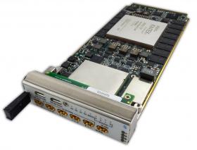
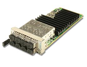
The VPX589 provides dual ADC sampling rates of up to 10.4/6.4 GSPS at a 12-bit resolution (TI ADC12DJ5200, ADC12DJ3200 or ADC12DJ2700) or quad inputs at 3.2 GSPS. Also, dual DAC delivers update rates of up to 12 GSPS and incorporates direct RF synthesis capable of 6 GSPS at a 16-bit resolution (Analog Devices AD9162 or AD9164). This makes VPX589 suitable for signal capture/analysis applications such as COMINT/SIGINT, radar, research and instrumentation.
The unit has an onboard Virtex UltraScale+™ XCVU13P FPGA that directly interface with ADC/DAC and a bank of 64-bit wide DDR4 memory channels with a total of 8 GB memory.
The module routes x16 SERDES to P1 which can run any protocol (i.e PCIe/SRIO/10G/40G/Aurora) and x8 SERDES with 16 LVDS signals to P2.
The unit is available in a range of temperature and shock/vib specifications per ANSI/VITA 47, up to V3 and OS2.
Please contact VadaTech for details of Conduction Cooled versions.
Key Features
- Xilinx Virtex UltraScale+™ XCVU13P FPGA
- Dual ADC 12-bit @ 10.4/6.4 GSPS or quad ADC @ 5.2/3.2 GSPS with TI ADC12DJ5200 or ADC12DJ3200
- Option for ADC12DJ5200, ADC12DJ3200 or ADC12DJ2700
- Dual DAC 16-bit @ 12 GSPS (AD9162 or AD9164)
- 16 SERDES as PCIe/SRIO/10GbE/40GbE/Aurora to P1
- 8 SERDES as PCIe/SRIO/10GbE/40GbE/Aurora to P2
- Clock Jitter cleaner
- Option for Direct RF Clock sampling for the ADC/DAC
- Single bank of DDR4 64-bit wide 8 GB Total
- Health Management through dedicated Processor
Benefits
- RADAR data processing
- Reference design with VHDL source code speeds application development
- Full system supply from industry leader
- AS9100 and ISO9001 certified company
Specifications
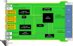
Block diagram
White Papers
Related Products
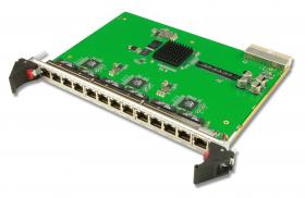
VPX516
3U FPGA Carrier for FMC, Xilinx Virtex-7, 3U VPX
- 3U FPGA carrier for FPGA Mezzanine Card (FMC) per VITA 46 and VITA 57
- Xilinx Virtex-7 690T FPGA in FFG-1761 package
- High-performance clock jitter cleaner
- VHDL reference design with source code
- Protocols such as PCIe, SRIO, 10GbE/40GbE, etc. are FPGA programmable
- Compatible with VadaTech and 3rd party FMCs
- 2.5 GB of DDR3 Memory
- Health Management through dedicated Processor
View product
VPX516 Data Sheet
VPX517
FPGA FMC Carrier, Xilinx Kintex-7, 3U VPX
- 3U FPGA carrier for FPGA Mezzanine Card (FMC) per VITA 46 and VITA 57
- Xilinx Kintex-7 410T FPGA in FFG-900 package
- High-performance clock jitter cleaner
- VHDL reference design with source code
- Protocols such as PCIe, SRIO, 10GbE/40GbE, etc. are FPGA programmable
- 2.5 GB of DDR3 Memory
- Compatible with VadaTech and 3rd party FMCs
- Health Management through dedicated Processor
View product
VPX517 Data Sheet
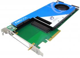
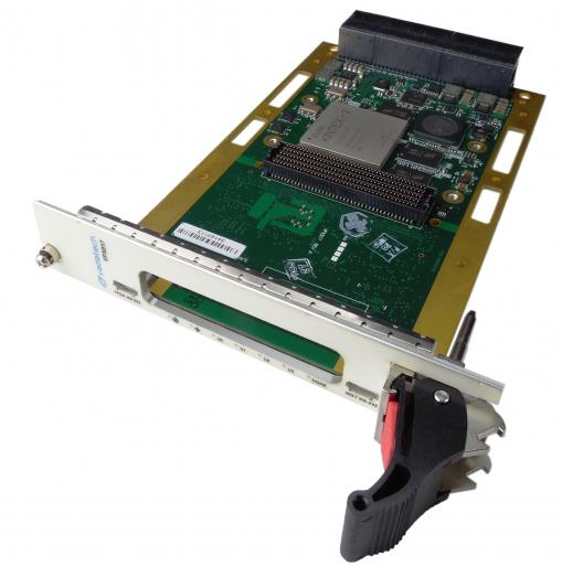
VPX592
FPGA/FMC Carrier, Kintex UltraScale™, 3U VPX
- 3U FPGA carrier for FPGA Mezzanine Card (FMC) per VITA 46 and VITA 57
- Xilinx Kintex UltraScale™ XCKU115 FPGA
- High-performance clock jitter cleaner
- VHDL reference design with source code
- Protocols such as PCIe, SRIO, 10GbE/40GbE, etc. are FPGA programmable
- Compatible with VadaTech and 3rd party FMCs
- 20 GB of DDR4 Memory (2 banks of 64-bit wide, and single bank of 32-bit wide)
- Health Management through dedicated Processor
View product
VPX592 Data Sheet
Info request
Create a list of products to inquire about for more information or quote request.