FPGA FMC Carrier, Xilinx Kintex-7, 3U VPX

  • 3U FPGA carrier for FPGA Mezzanine Card (FMC) per VITA 46 and VITA 57
  • Xilinx Kintex-7 410T FPGA in FFG-900 package
  • High-performance clock jitter cleaner can source P0_AUX_CLK to provide a common clock across the chassis.
  • VHDL reference design with source code
  • Protocols such as PCIe, SRIO, 10GbE/40GbE, etc. are FPGA programmable
  • 2.5 GB of DDR3 Memory
  • Compatible with VadaTech and 3rd party FMCs
  • Health Management through dedicated Processor

Download Datasheet Add to Info Request

add to compare

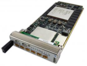
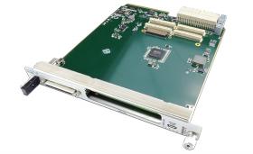
The VPX513 is a FPGA Carrier (VITA 46) with an FMC (VITA 57) interface. The unit has an onboard, re-configurable FPGA which interfaces directly to the FMC DP0-9 and all FMC LA/HA/HB pairs. The FPGA has interface to two DDR3 memory channels (64-bit wide and 16-bit wide) for a total of 2.5 GB. This allows for large buffer sizes to be stored during processing as well as for queuing the data to the host.

The clocking sub-system supports a common clock across GTX transceivers, which can be derived from an incoming GTX, sourced from an on-board oscillator (frequency selectable by ordering option), or taken from P0_AUX_CLK.  If sourced locally the clock can be driven back out through P0_AUX_CLK, supporting master/slave configurations to extend the common clock across a chassis.

The module supports dual GbE and, dependent on FPGA code loaded, PCIe up to Gen3 (dual x4 or x8 lane), or dual SRIO, 10GbE or 40GbE on P1.

The VPX513 provide health management through the dedicated management processor (including temp, voltage, FRU info, etc.).

The unit is available in a range of temperature and shock/vib specifications per ANSI/VITA 47, up to V3 and OS2.

Please contact VadaTech for details of Conduction Cooled versions.

Key Features
  • 3U FPGA carrier for FPGA Mezzanine Card (FMC) per VITA 46 and VITA 57
  • Xilinx Kintex-7 410T FPGA in FFG-900 package
  • High-performance clock jitter cleaner can source P0_AUX_CLK to provide a common clock across the chassis.
  • VHDL reference design with source code
  • Protocols such as PCIe, SRIO, 10GbE/40GbE, etc. are FPGA programmable
  • 2.5 GB of DDR3 Memory
  • Compatible with VadaTech and 3rd party FMCs
  • Health Management through dedicated Processor
Benefits
  • Uses same frequency source across multiple GTX blocks for backplane & FMC
  • Reference design with VHDL source code speeds application development
  • Electrical, mechanical, software, and system-level expertise in house
  • Full system supply from industry leader
  • AS9100 and ISO9001 certified company
Specifications
Specifications

Block diagram

Related Products

FMC109

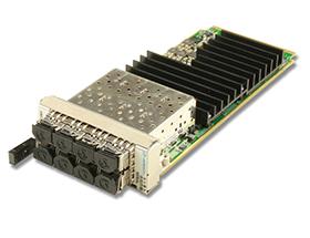
FMC QUAD SFP/SFP+ for GbE/10GbE

  • FPGA Mezzanine Card (FMC) per VITA-57
  • Single module
  • Quad SFP/SFP+ cages for quad ports
  • Re-driver on all four ports for a better signal quality
  • RoHS compliant
View product FMC109 Data Sheet

FMC211

FMC High-speed ADC 10-bit at 2.6 GSPS Module

  • FPGA Mezzanine Card (FMC) per VITA-57
  • ADC EV10AS150B  @ 2.6 GSPS
  • 5 GHz Full Power Input Bandwidth (–3dB)
  • True single core architecture (no calibration required)
  • Full scale Analog input Voltage Span 500 mVpp
  • Ultra Low Jitter wideband PLL Synthesizer
  • Option for Direct RF clock sampling or  reference clock input
  • The ADC RF input can be differential or single ended
View product FMC211 Data Sheet

FMC228

Quad ADC 12-bit @ 1 GSPS, FMC

  • FPGA Mezzanine Card (FMC) per VITA 57
  • Quad ADC based on AD9234 (1 GSPS or 500 MSPS)
    • Optional decimate-by-2 DDC per channel
    • JESD204B
    • 2 GHz analog input full power bandwidth
  • Option for Direct RF sampling clock via front panel
  • Supported by DAQ Series™ data acquisition software
  • On board wide-band PLL
  • Trig In/Out
  • CLK In
View product FMC228 Data Sheet

Info request

Create a list of products to inquire about for more information or quote request.