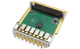
3rd Generation RFSoC w/ XCVU13P FPGA and RF/IF carrier
- 8 ADC / 8 DAC simultaneous processing
- 3rd Generation Xilinx RFSoC XCZU47DR
- Suitable for 5G, 4G, LET and SDR deployment
- FPGA data processing w/ Xilinx Virtex UltraScale+ XCVU13P
- FMC+ socket for addition RF and I/O
- The FMC+ could extend beyond the FMC+ in length for added real estate (up to XMC size is supported)
- Accommodate 3rd party RF/IF daughter card
- Accomplished thru an FMC connector to the RF Module
- Clock and Timing Synchronization to the RF/IF
Download Datasheet Add to Info Request
add to compare
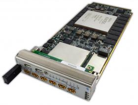
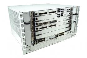
The VT981 is a complete data acquisition and processing platform capable of synchronous sampling, suitable for customer development of custom RF front end. It has 8 channels ADC and 8 channels DAC embedded in the 3rd generation RFSoC XCZU47DR with bandwidth up to 800MHz from DC to 6GHz. The RFSoC provides clock and frame synchronization signals to the RF/IF Daughter Card, the DSP FPGA, and external Control Module. .
The RFSoC has 8GB 64-bit DDR4 with ECC to the CPU and 8GB 64-bit DDR4 to the Fabric side. The Xilinx ZCVU13P has 16GB 64-bit DDR4 (two banks of 8GB) on-board memory. Both XCZU47DR and the XCVU13P have JTAG and serial via the front dual USB connectors.
The RFSoC interface includes CPRI over SFP+ on the front panel and the FPGA XCVU13P supports six 100GbE interfaces via QSFP28 on the front panel.
The VT981 has a Layer 2 Managed Gigabit Ethernet Switch with dual GbE (RJ‑45) and single 10GbE (SFP+) interfaces to the front panel, providing interconnection among the subsystems.
VT981 has an option for an FMC+ module which interfaces to the VU13P FPGA. The module mounted here can be larger than the FMC+ specification to extend the area available for components, allowing up to an XMC module size. The XCZU47DR RF is routed to an interface connector with an additional FMC style connector for control to a customer RF front-end module.
The VT981 has a dedicated CPU for health management. The health management CPU monitors the sensors in the chassis and controls the cooling dynamically. The cooling is from right to left.
The chassis mounting provision allows the unit to be in a 19” rack or ceiling mounted.
Key Features
- 8 ADC / 8 DAC simultaneous processing
- 3rd Generation Xilinx RFSoC XCZU47DR
- Suitable for 5G, 4G, LET and SDR deployment
- FPGA data processing w/ Xilinx Virtex UltraScale+ XCVU13P
- FMC+ socket for addition RF and I/O
- The FMC+ could extend beyond the FMC+ in length for added real estate (up to XMC size is supported)
- Accommodate 3rd party RF/IF daughter card
- Accomplished thru an FMC connector to the RF Module
- Clock and Timing Synchronization to the RF/IF
Benefits
- Design utilizes proven VadaTech subcomponents and engineering techniques
- Electrical, mechanical, software, and system-level expertise in house
- Full system supply by industry leader
- AS9100 and ISO9001 certified company
Specifications
Block diagram

Related Products
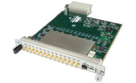
AMC521
24 Channels ADC, Mixed Sampling Rate
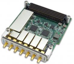
- Sixteen channel of TI ADS42JB69 ADC 16-bit @ 250 MSPS
- Eight channel SAR TI ADS8568 ADC 16-bit @ 650 KSPS simultaneous
- Interface to the FPGA via JESD204B
- 24 LVDS for Clock/Trig and/or GPIO
- Virtex-7 FPGA 415T or 690T in FFG1158
- Internal/External clock
- Clock Jitter Cleaner with Dual Loop PLLs
- Trig In/Out
- A/D input via SSMC connectors
View product
AMC521 Data Sheet
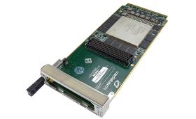
AMC524
Quad ADC, 16-bit @ 125 MSPS, Dual DAC, Artix-7
- Quad ADC 16-bit @ 125 MSPS (AD9653)
- Dual DAC 12-bit @ 2.5 GSPS (DDS AD9915)
- Artix-7 FPGA with dual banks of DDR3, 2 GB total
- Conduction cooled version available
- Internal, external or backplane clock with onboard Wideband PLL
- AMC Ports 4-7 and 8-11 are routed to FPGA per AMC.1, AMC.2 and AMC.4 (PCIe, SRIO, XAUI, etc. are FPGA programmable)
- Single module, mid-size per AMC.0
- IPMI 2.0 compliant
View product
AMC524 Data Sheet
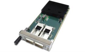
AMC526
AMC Dual ADC, Virtex-7, 12-Bit @ 2.6 GSPS
- Single module, mid-size per AMC.0
- Conduction cooled version available
- Dual ADC, 12-Bit @ 2.6 GSPS (AD9625) in single module, mid-size
- Xilinx Virtex-7 690T FPGA in FFG-1761 package
- Quad bank QDR-II+ memory (576 Mb total) and 1Gb DDR3
- AMC Ports 4-11 are routed to FPGA per AMC.1, AMC.2 and AMC.4 (PCIe, SRIO, XAUI, etc. are FPGA programmable)
- AMC Ports 12-15 and 17-20 optionally routed to the FPGA
- Internal, external or backplane clock with onboard Wideband PLL
- IPMI 2.0 compliant
View product
AMC526 Data Sheet
Info request
Create a list of products to inquire about for more information or quote request.
