I accept VadaTech copyright information.
Home
Products









Newsroom
By Function


 |
I accept VadaTech copyright information.
Please enter your email registered at VadaTech and we will send you your password.
Download Datasheet Add to Info Request
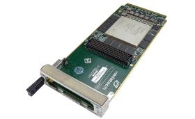
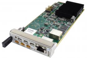
add to compareThe XMC502 is an XMC module per VITA 42 specification and based on the Xilinx Kintex Ultrascale+ FPGA XCKU11P. The XMC502 interfaces to the host via x8 PCIe Gen3 (other protocols such as 1G/10G/40G, Aurora, SRIO, etc. are possible by programming the FPGA).
The XMC502 has dual bank of DDR-4 memory (32-bit wide) for a total of 8GB of memory.
The module follows the VITA 46.9 and routes I/O to XMC P16/P14 as P64s+X24s+X8d+X12d. Two of the X24s are used for the 1PPS and sine wave input as sync clock to the on board PLL. There are six LVDS input/output (could be configured in any combination as single ended +1.8V) and ten GPIO +3.3V. Ten of the X12d are high speed SERDES that connect directly to the MGT Bank of the FPGA. P64s are all configured as +3.3V.
The 10 high speed SERDES going to the P16 could be configured for PCIe or non-PCIe protocols. There are two hard core PCIe and some of the valid PCIe configuration are show below:
There are many other combinatorial to take advance of smaller PCIe lanes to add more lanes to the non-PCIe protocols such as:
Please contact VadaTech for other configurations.
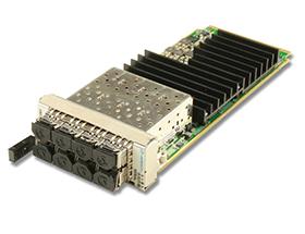
The module has an option for the front panel Optical via SFP+ (SFP28) style which can operate up to 25G per lane. This allows operations such as 25Gb ethernet or 100G across four optics. Since the FPGA is programable any protocol could be run on these lanes with mix and match including PCIe, Aurora, etc.
The XMC502 has an on board PLL which can generate any frequency to the MGT banks. The PLL can lock into a 1PPS or 10Mhz (or any sine wave input up to 300MHz) clock. The sync clocks have their input thru the front panel or thru the P16 connectors. User can select the sync input and the priority. The XMC502 could still operate and generate any clock to the MGT without any sync reference clock.The PLL has hitless fail over its input sync clocks.
The PLL has an OCXO for stability reference and XO as the jitter reference.
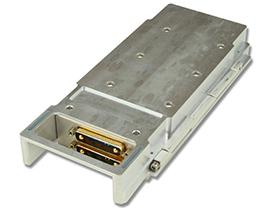
The module is available in both air cooled and conduction cooled versions.