I accept VadaTech copyright information.
Home
Products

Newsroom
By Function


 |
I accept VadaTech copyright information.
Please enter your email registered at VadaTech and we will send you your password.
Download Datasheet Add to Info Request
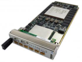
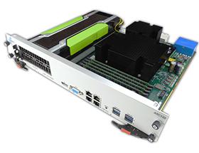
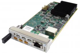
add to compareThe AMC541 is based on the Xilinx Zynq® Ultrascale+ XCZU19EG MPSoC FPGA with embedded Quad-core ARM Cortex-A53 application processing unit, Dual-core ARM Cortex-R5 real-time processing unit, ARM Mali - MP2 GPU. The FPGA has Dual banks of 64-bit DDR4 memory (one bank to the ARM Core and one bank to the FPGA) and includes an SD card.
The AMC541 has the TCI6638K2K communications infrastructure KeyStone SoC, which is a member of the C66x family based on TI’s new KeyStone II Multicore SoC Architecture, designed specifically for high-performance telecommunication, IoT and networking applications. It features eight TMS320C66x DSP core subsystems (C66x CorePacs). The TMS320C66x interfaces to dual 64-bit wide DRAM DDR3.
The flexible architecture including multiplexer allows the FPGA and DSP to interface to the AMC connector in different configurations. The AMC connector Ports 2-3 and 8-11 are linked directly to the FPGA for the core to interface with the host through multiple protocols such as SRIO, PCIe or 10/40GbE. Ports 4-7 can connect directly to the FPGA in addition to Ports 8-11 or connect directly to the DSP with SRIO protocol via MUX selection (DIP-switch selection).
The module also routes GbE on Ports 0 and 1 per AMC.2. The DSP and FPGA are linked via PCIe x2 and GbE.
The onboard, re-configurable FPGA interfaces to the AMC FCLKA (fabric clock) and TCLKA-D (user clocks and triggers) via a clock and jitter cleaner. The module also has a front panel TRIG IN and CLK IN to the clock and jitter cleaner.
The front panel SFP+ cage allows expansion via fiber 1/10GbE or 1/10GbE copper interface.